EFA 4M50HL3 The Retro Web User Manual
- June 15, 2024
- EFA
Table of Contents
EFA 4M50HL3 The Retro Web

All other products or services are identified by he trademarks or service marks of their respective company. IBM and PS2 are registered trademarks of Internation Business Machines Corporation. Microsoft and MS-DOS are registered trade mark of Microsoft Corporation.
Introduction
The 486 Interchangeable Mother Board 4M50HL3
4M50HL3 is truly an universal mother board for all occasions-the mother of all
mother boards. The sockets that can accommodate 486 series of CPU chips,
4M50HL3 allows the user to interchange the CPU chip on board any time he
chooses to. With the help of changing a few jumper wires additionally, one can
literally re- configure one’s PC system from a low end 80486SX at 20MHz to a
high end 80486DXat50MHzanytirneonechooses. The economy and simplicity of
upgrading or re-configure of the user’s PC system, by only unplug ginga CPU
chip plus changing a few jumper wires, offers all kinds of ways to save and to
expand in numerous applications!
Specifications
- Model: 4M5011L3
- Mainboard: 4DMU=50HL3-L4-VB
- Processor: Intel or AMD CYRIX microprocessor (80486SX, P24T, M6, C6, 80486DX2-66/50, and 80486DX20MHz, 25MHz, 33MHz, 40MHz, 50MEIz)
- Cache memory: Optional 64KB,128KB or 256KB cache memory
- Main memory: Cacheable 32MB main memory
Features
General Specifications and Features
The 4M50HL3 mainboards are based on the powerful 80486SX/DX/DX2
microprocessor, respectively, and incorporate advanced computer technology to
meet the requirements of the next generation of operating systems and
applications. Yet they retain full compatibility with the original IBM PC XT
and AT and use existing PC software and hardware.
-
Intel or AMD CYRIX microprocessor: 80486SX, P24T, M6, C6, 80486DX2-66/50, and80486DX20I\1Hz, 25MHz, 33I\1Hz, 40MHz, 50MHz.
-
Built-in cache controller
-
Optional 64KB, 128KB or 256KB cache memory allowing the CPU to. run at full speed most of the time. Cacheable 32MB main memory.
0 wait state for cache read/write hit. Hidden DRAM refresh cycle to boost system performance. Built-in registers to support three independent non- cachable memory area Supports interleaved cache RAM for high speed CPU. Supports cache line fill as well as 80486 burst mode. Cache enable/disable and programmable non-cacheable memory area via software setup. -
Sophisticated DRAM controller
-
Supports fast/standard page mode.
-
Supports two bank of SIMM sockets with up to 32MB of total memory.
-
Flexible DRAM memory configuration to accommodate from 1 MB t 32MB in different options of memory size by using a combination of 256K.Bx9, 1Mx9,4MBx9, lMBx3,DRAM SIMM modules. 4M50HL3 User’s Manual 1-2
-
Programmable DRAM wait states.
-
Intelligently relocation the 256KB or 3 84KB memory block up from the reserved 384KB memory space to the top of DRAM memory.
-
Support automatic memory size detection.
-
Single ROM BIOS support, default 64 KB AMI BIOS with built-in Setup program.
-
Complementary metal oxide semiconductor ( CMOS) RAM to maintain system configuration.
-
CPU clock by DIP switches setting.
-
Supports fast A20 Gates and fast CPU reset to boost performance of software utilizing 80486 protected mode, such OS/2, UNIX … etc.
-
Support parity generation and checking.
-
Eight ISA expansion slots: Seven 16-bit slots one 8 bit slot for AT-compatible add-on cards.
-
Three VESA-Local bus slots. Slave/Master mode.
Major Components
The4M50HL3 mainboards are composed of many integrated circuits. Chips. The
major components and their basic features are outlined as below.
- UM82C48 l Itegrated Memory Controller (IMC)
- UM82C482 Integrated System Controller (ISC)
- UM82C206 Itegrated Peripheral Controller (IMC)
- VISA Local Bus
- The4M50HL3 board support VISA local bus Slave/Master mode.
Pin assignment list belows
| Pin | Assignment | Pin | Assignment | Pin | Assignment | Pin | Assignment |
|---|---|---|---|---|---|---|---|
| Pl | PDl | P29 | PAIS | P59 | PD0 | PS7 | GND |
| P2 | PD3 | P30 | PA16 | P60 | PD2 | PSS | PA17 |
| P3 | GND | P31 | PA14 | P61 | PD4 | PS9 | PA15 |
| P4 | PD5 | P32 | PA12 | P62 | PD6 | P90 | vcc |
| P5 | PD7 | P33 | PAl0 | P63 | PDS | P91 | PA13 |
| P6 | PD9 | P34 | PAS | P64 | GND | P92 | PAll |
| P7 | PDll | P35 | GND | P65 | PDl0. | P93 | PA9 |
| PS | PD13 | P36 | PA6 | P66 | PD12 | P9A | PA7 |
| P9 | PD15 | P37 | PA4 | P67 | vcc | P95 | PAS |
| Pl0 | GND | P3S | N/C | P6S | PD14 | P96 | GND |
| Pll | PD17 | P39 | PBE*0 | P69 | PD16 | P97 | PA3 |
| P12 | vcc | P40 | vcc | P70 | PDlS | P9S | PA2 |
| P13 | PD19 | P41 | PBE*l | P71 | PD20 | P99 | N/C |
| P14 | PD21 | P42 | PBE*2 | P72 | GND | Pl00 | LRESET* |
| P15 | PD23 | P43 | GND | P73 | PD22 | Pl0l | PDC |
| P16 | PD25 | P44 | PBE*3 | P74 | PD24 | P102 | PMIO |
| P17 | GND | P45 | PADS* | P75 | PD26 | P103 | PWR |
| PlS | PD27 | P46 | WIKRDY* | P76 | PD2S | P106 | PRDY* |
| P19 | PD29 | P49 | CLBA* | P77 | PD30 | P107 | GND |
| P20 | PD31 | P50 | LREQ* | P78 | vcc | Pl0S | IRQ9 |
| P21 | PA30 | P51 | GNE | P79 | PA31 | P109 | BRDY* |
| P22 | PA28 | P52 | LGNT* | PS0 | PA29 | P110 | BLST* |
| P23 | PA26 | P53 | vcc | PSl | GND | Plll | ID0-1 |
| P24 | GND | P54 | ID2-1 | PS2 | PA27 | P112 | IDl-1 |
| P25 | PA24 | P55 | ID3-1 | PS3 | PA25 | P113 | GND |
| P26 | PA26 | P56 | ID4 | PS4 | PA23 | P114 | JP02 |
| P27 | vcc | P57 | KET* | PS5 | PA21 | Pll5 | VCC |
| P2S | PA20 | P5S | PEADS* | PS6 | PA19 | P116 | LSV16* |
Memory Configuration
DRAM Banks Configuration
The 2 banks are composed of 8 standard 30-pin SIMM sockets. These sockets
take 256-KB, 1-MB or 4-MB SIMM. (It can be a mix or these SIMMS). In table
2.1, all the possible combination of the DRAM modules to make up from 1-MB to
32-MB as the total amount of memory for the system are listed. For better
performance, We do recommend quality 70ns. SIMM for 486DX 33.MHz boards and
80ns SIMM for 486SX20.MHz.
Memory Configuration
| BANKO | BANKl | TOTAL MEMORY |
|---|---|---|
| 256K | —— | lM |
| 256K | 256K | 2M |
| 256K | lM | SM |
| lM | —– | 4M |
| lM | lM | 8M |
| lM | 4M | 20M |
| 4M | —– | 16M |
| 4M | 4M | 32M |
Note: Memory counting during the Power-on self test (POST), The memory count shown on the screen does not include the shadow RAM area ( 128K).
The following formula illustrates how the total memory comes out
Memory count on the monitor= Installed total memory 384KB + Relocation memory.
For example, the user installed a total of 4MB on board and relation the
256-KB/3 84-KB memory. In this case, the total memory displayed on the screen
will be3968-KB/384-KB.
To relocation the unused 256-KB/3 84KB of reserved memory above normal
extended memory, you could enable the main memory relocation option in the
CMOS SER UP menu. To run the SETUP program and enable the main memory
relocation function, refer to Chapter 4 for details
Cache Memory Subsystem
The mainboard supports optional cache memory of 64KB, 128KB, or 256KB. This
cache memory allows the CPU to run at full speed most of the time. It also
offers cacheable 32MB main memory and provides 0 wait state for cache
read/write hit. Additionally, it has a hidden DRAM refresh cycle to boost
system performance. The mainboard also has built-in registers to support three
independent non-cacheable memory areas. It supports interleaved cache RAM for
high-speed CPU and cache line fill as well as 80486 burst mode. The cache
memory can be enabled or disabled and the non-cacheable memory area can be
programmed via software setup. The 4M50HL3 accept optional 64KB, 128KB or
256KB or SRAM for cache memory support. The SRAM chip shousd be 8Kx8bit or
32Kx8bitwith speed of25nsforthe486SX20MHz,20nsfor486DX33/50MHz. The TAGRAM (Ul
7) is for saving address and compare the next CPU address. A TA GRAM should be
used ap speed 20ns for the 486DX. The table below list all the possible SRAM
location and the total amount of Cache RAM memory for each option.
SRAM Configuration
Option| BANKO U24, U25, U26,U27| BANKl U34,U35,U36,U37| Cache Memory Amount|
TAG RAM (Ul7)
---|---|---|---|---
1| 8K x 8bit SRAM| 8K x 8bit SRAM| 64K| 8Kx 8
2| 32K x 8bit SRAM| 0| 128K| 8Kx 8
3| 32K x 8bit SRAM| 32K x 8bit SRAM| 256K| 32Kx 8
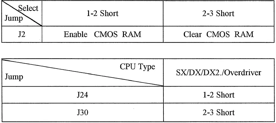
Jumper Settings and Connectors
This chapter will assist you with setting-up the 4 M5 OHL3 before you install it in a system case. If your 4M50HL3 has already been installed and you do not wish to change the configuration settings, you can skip over this section.
Jumper Switches
The 4M50HL3 has several jumper switches that must be set to define a system
configuration. These Jumper are three-pin components on the · mainboard. They
are turned off and on by placing or removing a cover cap over the pins. This
is called a open or closed jumper. All jumpers must be set to one of the two
possible settings.
Cache RAM Jumper Setting
CAC SIZE| Jl6| Jl5| J8| J7| Jl2| Jll| no|
J9| CACHEABL RANGE
---|---|---|---|---|---|---|---|---|---
64K
Byte| 1.2| 1.2| 2.3| Open| Open| Open|
Open| Open| 16MB
128K
Byte| 2.3| 1.2| 1.2| 2.3| Open| Close|
Open| Close| 32MB
256K
Byte| 2.3| 2.3| 2.3| 1.2| Close| Close|
Close| Close| 64MB
Note
- 64K byte= 8 pieces of 8K x 8 SRAM on cache bank O and 1
- 128K byte= 4 pieces of 32K x 8 SRAM on cache bank 0
- 256K byte= 8 pieces of 32K x 8 SRAM on cache bank O and 1
486SX Switch Setting (PGA Packing)
Switch 1 Configuration CPU Speed Select
| SWI-1| SWI-2| SWI-3| SWI-4
486SX-20| OFF| OFF| ON| OFF
486SX-25| ON| ON| OFF| ON
486SX-33| ON| OFF| ON| ON
M6| OFF| OFF| ON| OFF
Jumper Configuration CPU Type Select
| Jl8| Jl9| J20| J21
486SX-20| Open| Open| Short| Short
M6/486SX-25/33| Open| Open| Open| Short
Other
Jumperb J17| Open
486DX Switch Setting
Switch 1 Configuration CPU Speed Select
| SWl-1| SWl-2| SWl-3| SWl-4
486DX-25| ON| ON| OFF| ON
486DX-33| ON| OFF| ON| ON
M7 I 486DX-40| OFF| OFF| ON| OFF
486DX-50| OFF| OFF| OFF| OFF
Jupmer Configuration CPU Type Select
| J18| Jl9| 120| J21
M7 I 486DX SERIAL| Short| Short| Open| Open
Other
Jumper 17| 1-2 Short
486DX2 Switch Setting
Switch 1 Configuratio CPU Speed Select
| SW 1-1| SW 1-2| SW 1-3| SWl-4
---|---|---|---|---
486DX2-50| ON| ON| OFF| ON
486DX2-66| ON| OFF| ON| ON
Other
486DX2 Serial| J18| J19| J20| J21
486DX2 Serial| Short| Short| Open| Open
Jumper 17| 1-2 Short
CYRIXM6 with C6 Switch Setting
Switch 1 Configuration CPU Speed Select
| SWl-1| SWl-2| SWl-3| SWl-4
M6+C6 (33MHz)| ON| OFF| ON| ON
M6+C6 (40MHz)| OFF| OFF| ON| OFF
Jupmer Configuration CPU Type Select
| J18| J19| J20| J21
M6+C6 Serial| Short| Short| Open| Open
Other
Jumper J17| 1-2 Short
CPU Type /Jumper| W/CYRIX C6| W/0 CYRIX C6
Jumper 14| Short| Open
Jumper 13| 2-3 Short| 1-2 Short
VL-BUS Jumper Setting
J23: VL-BUS FAST write wait state
| Fast Write Wait | J23 |
|---|---|
| OWAIT | User Select Mode l-2short |
| 1 WAIT | User Select Mode 2-3 short |
J22,J6: CPU Speed select
| CPU SPEED | J22 | ]6 |
|---|---|---|
| <=33MHz | 1-2. | 1-2 |
| >33MHz | 2-3 | 2-3 |
Other Jumper Setting


Nort: If use WESTERN DIGITAT HDD NO: WDAC2340 please set J5-2-3 short.
Connectors
There are several connectors located on the 4M50HL3. They are used to
connect with some peripheral devices to enhance the performance of the system
operation. Refer to APPENDIX B for the positions of all the connectors on the
mainboard.
Their functions are listed below
| Connector | Function |
|---|---|
| JI | External Battery Connector |
| J27 | Keylock Connector, Power LED Connector |
| J26 | Speaker Connector |
| J28 | Hardware Reset Connector |
| KBI | Keyboard Connector |
| PSI | Connectors the Power Supply |
| J25 | Turbo LED Connector |
The following lists the pin assignments for each connectors
External Battery Connector (Jl)
Pin No.| Assignment| Pin No.| Assignment
1| +3.6 VDC| 3| GND
2| Not Used| 4| GND
Turbo LED Connector (J25)
1| +5V| 2| Turbo
Hardware Connector (J28)
1| RESET| 2| GND
Speaker Connector (J26)
1| Data IN| 3| GND
2| Not Used| 4| +5V
Keylock Connector (J27)
1| +VDC| 4| Keylock
2| NC| 5| GND
3| GND| |
Keyboard Connector (KBl)
1| Keyboard LOCK| 4| GND
2| Keyboard DATA| 5| vcc
3| Not Used| |
Power Connector (PSl)
1| Power Good| 7| GND
2| +5V| 8| GND
3| +12V| 9| -5V
4| -12V| 10| +5V
5| GND| 11| +5V
6| GND| 12| +5V
Setup
Built-in BIOS Setup program
This chapter provides detailed instructions on how to configure your system
using the Built-in BIOS Setup Program and gives some technical information
about your computer. If you are not very familiar with micro computers, please
carefully read this chapter before proceeding. If you do not want to change
the system’s configuration, you can skip this chapter. SETUP program built in
the system BIOS.
How to Recall the Setup Program
You can run the built-in SETUP program in several ways
When powering-on the system
When you tum on the system power, or press the button on the system case while
the system is running (not every system has this button), the BIOS will first
test the functionality of the system components and display a start-up message
similar to the following
XXXKB OK
Hit key if you want to run setup
The numeral digits will continue to count at the top left of the screen. This
is the BIOS testing the mainboard memory chips. Before the above · message
disappears, you can, press the key to run the Setup program.
To reset the system
By pressing key combination when the system is up and
running (assuming you are running under DOS or other environments that support
this feature), the system will immediately reset itself and boot up. Before
booting up from a . diskette or hard disk, you can also see the below start-up
message
Hit key, if you want to run setup
When the BIOS Prompts you
In the self-test process, if the BIOS detects inconsistent or incorrect
configuration information, or some physical system error, it will display an
error message on the screen, and prompt you to take action; for example:
RUN SETUP UTILITY
- Press the
to RESUME - Press the
key, and continue.
To Enter password
If you set the password checking option to the. “Setup” or” Always” field in
the Advanced CMOS Setup program, after pressing the key to run he Setup
program, it will display the Enter password message on the screen. Refer to
section 5.6, Using Change Password Setup. The default password setting is
“
Running the Setup Program
When you call up the Setup program, the screen displays a’ ‘main menu”
similar to the following
BIOS Setup Main Menu Options
On-screen instructions at the bottom or the screen explain how to use the
program.
Using the Setup main menu
The following table describes available keys in the SETUP main menu
| Key | Usage |
|---|---|
| ESC | To exit without saving and reboot the machine |
| To move the selection bar around | |
| F2 I F3 | To change color |
| F 10 | To save changes and reboot the machine |
The following is a brief description of the six options of the Setup main menu
STANDARD CMOS SETUP
Display the standard CMOS Setup screen to check or modify general
configuration information. The standard CMOS setup for the date, time, floppy
type, hard disk type, video type, etc.
ADV AN CED CMOS SETUP
The ADVANCED CMOS SETUP option is used to set the various, system options for
the user, including the above 1 MB memory test, Scratch RAM area for BIOS,
Co-processor detection, Video ROM Shadow and System ROM Shadow.
ADVANCEDCHIPSET SETUP
This Setup Option is for the user who wishes to program the chip set
registers. The chip set registers control most of the system options in the
computer.
AUTO CONFIGURATION WITH BIOS DEFAULTS
This option allows for automatic configuration of all the options in the
Advanced CMOS Setup/ Advanced Chipset Setup with the BIOS defaults.
CHANGE PASSWORD
The Password is required for entering the Setup Program or boot your system.
The user can Change the ROM default or current (user) password stored in the
CMOS by accessing this option. The ROM default password is the “AMI” string:
When you want to use this option, you must be enabled the password option in
ADVANCED CMOS SETUP.
WRITE TO CMOS AND EXIT
Choose this option to save the changes you have made in the “Standard Setup”,
“advanced Setup” and “Advanced Chipset setup” option, and then exit to -reboot
the system.
DO NOT WRITE TO CMOS _AND EXIT
Choose this option to all abandon all previous settings and then exit to
reboot the system, To choose an item from the setup main menu, move the cursor
to appropriate line using the Up <↑> and Down<↓> arrow keys and press
The screen will display a warning message as below

Running the standard CMOS Setup
To check or modify the general system configuration, choose “STANDARD CMOS
SETUP” from the Setup main menu and press

The Standard CMOS Setup Program Screen
One-screen instructions in the lower left comer of the screen explain how to
use the program. After making all selections, Press
Using the Standard CMOS Setup Program
| Key | Usage |
|---|---|
| To move the selection bar around | |
| PgUp/PgDn | To modify the values of the option by scrolling through the |
predefined values in most fields
F2/F3| To change color
Enter| To move teh selection bar around
ESC| To exit to previous screen
Date
In the Date fields, you manually set the electronic calendar on the main
board only if the values are incorrect.
Time
Time fields include hour, minutes, seconds, but you can only set the value of
hour and minute. Check and adjust these fields as you would a clock or wrist
watch.
Daylight saving
In this field you can enable or disable the daylight saving function.
Floppy Drive A and B
In this field you may specify the capacity and format of the floppy drives
installed in your system.
- 360KB,5-l/4″
- 1.2MB, 5-1/4″
- 720KB, 3-1/2″
- 1.44 MB, 3-1/2″
- 2.88MB,3-l/2″
- Not Installed
Hard Disk C: and Hard Disk D:
In these fields, you specify the physical and electronic properties of the
“Standard” hard disk drives installed in your system. Relevant specifications
include the number of cylinders and heads, write pre-compensation time,
read/write head landing zone, number of sectors per track. The BIOS provides
46 predefined types of popular hard disk drives. You select the appropriate
type by scrolling forward/backward using the
. (Sectors) fields and directly key in the appropriate values. The Setup
program will calculate the capacity of the drive based on the input cylinder,
head and sector numbers and display the result on the capacity field for your
reference.
Refer to Appendix A for the table of hard disk types.
Primary Display
In the display field, you specify the display adapter installed in your
system.
Keyboard
This setting· is used to select “Installed” or “Not Installed” for the
keyboard during to Power On Self Test. Normally, it should be set as
”Installed”.
Base Memory and Extended Memory Size
A small section in the upper right comer of the screen displays important
status information on your system, including base and extended memory amount.
They are updated automatically by the Setup program according to status to
status detected by the BIOS self-test; no manual change is allowed.
Running the Advanced CMOS Setup
When you choose the ” RUN Advanced CMOS Setup” option in the Setup main
menu, the screen displays the following menu

The Advanced CMOS Setup Program Screen
Using the Advanced CMOS Setup Program
| Key | Usage |
|---|---|
| To move the selection bar around | |
| PgUp/PgDn | To modify the values of the option by scrolling through the pre- |
defined values in most fields
Ctrl+PgUp/PgDn| To quickly modify the values of the Option by scrolling
through the predefined values in the “Non-Cacheable Base & Size” field.
Fl| To get help for each of the options
F2/F3| To change color
F5| To get the old values. These values are the values which the user
started the current session with. If the CMOS was good, then the old values
are the CMOS values; otherwise they are the BIOS Setup default values.
F6| To load all the options in the Advanced CMOS Setup/ Advanced Chipset
Setup with teh BIOS Setup default.
F7| To load all the options in the Advanced CMOS Setup/ Advanced Chipset
Setup with the Power-On default.
ESC| To exit to previous screen i
Hard Hard Disk Type 47 RAM Area
The purpose of this field is to specify the address of the memory area used by
the system BIOS for storing extended information, such as to save the user
definable drive type 47.
You have the following options
-
0:300
To reserve the stack area at address 0:300H -
DOS 1KB
To reserve the top 640 KB in the DOS base memory and reduce the size of base memory by 1 KB. The default is option “0:300H”.
System Boot Up Num Lock
This option can set the “Num Lock ” key to “On” or “Off’ after system boot up.
Cache Memory
Due to constraint of technology, speed of currently available DRAM may not be
high enough to catch up with the speed of the CPU, which means that at every
setup of program execution, the CPU must wait for the DRAM to response. In
fact, CPU to run faster, the system must be designed to use another kind of
fast RAM chip – SRAM (Static-column RAM).
In 4MS0HL3, you can have a dual cache architecture -internal (from the CPU) &
external cache (from the SRAM).
The options are as follows
- Disable
- Internal
- BOTH
You should usually setting the “BOTH” option to get full potential of the system when you using a 486 DX CPU. You have to setting the “BOTH” to 486DLC CPU (Because 386 CPU have not internal cache RAM).
Gate A20 emulation
Press F 1 the screen display the following explanation
Gate A20 Emulation
Disabled: Gate-20 is controlled by keyboard controller(8042)for programs
which uses BIOS calls as well as for programs which uses VO ports.
Chipset: Gate-20 is controlled by chipset (UMC82C482A) for programs which
uses BIOS calls as well as for programs which uses VO ports 60H/64H for
doing Gate-A20 operations.
Fast : Gate-20 is controlled by VO port 92H for programs which uses
BIOS calls for doing Gate-A20 operations. For programs which uses 1/0 ports
60H/64H for doing Gate-A20 operations Gate-A20 is controlled by keyboard
controller (8042).
Both : Gate-A20 is controlled by I/O port 92H for programs which uses
BIOS calls for doing Gate-A20 operations. For programs which uses I/O port
60H/64H for doing Gate-A20 operations Gate-A20 is controlled by chipset
(UM82C482A).
Available Options:

Note:
Also you can pressing the
Password Checking Option
The purpose of this field is to determine whether the password is asked for in
every boot (set to “Always”) when entering into the Setup program (user to
“Setup”) or never (set to “Disabled”).
Video ROM Shadow
Choose these two options for better video display performance. It enables the
shadow RAM operation for the video BIOS on display cards such as VGA or EGA.
The Video card should be checked to see whether it has 16K or 32K of ROM. _ If
there is no ROM in the display card, there is no need to shadow the Video
BIOS. If is has 16K of ROM, the Video BIOS should be shadowed at C000, 16K. If
the card has 32K of ROM, the Video BIOS should be shadowed at both C000, 16K
and C400, 16K.
Running the Advanced Chipset Setup
To program the registers of the CHIPSET, choose the “Advanced ChipSet
Setup” option from the Setup main menu and press

The Advanced Chip S et Setup
Non-Cacheable Block Size and Address
For some special I/O card need to use system memory, you should reserve space
of the memory for its use. There is two continuous address areas for Non-
cacheable blocks in the 4M5OHL3. The options ofNon-cacheable Block-1 size.
- Disabled
- 4KB
- 8 KB
- 16 KB
- 32 KB
- 64 KB
- 128 KB
- 25 6 KB
- IMB
According to the above non-cacheable block-1 size setting, you should set the proper address.
- 64}(J3
- 128 KB
- 512 KB
- 1 MB
- 2MB
- 4MB
- 8MB
- 16 MB
F000 Memory, 64K Cacheable
If you have shadowing of the system BIOS, you can enable this option for
memory cacheable function.
C400 Memory, 16K Cacheable
If you shadowing the video BIOS at C400, 16K, you can enable this memory
cacheable function.
AMIBIOS SETUP PROGRAM – ADVANCED CHIPSET SETUP
(C)1992 American Megatrends Inc., All Rights Reserved
IDE Standby mode : Present
ESC: Exit Sel (Ctrl) Pu/Pd: Modify F1: Help F2/F3: Color
F5: Old Values F6: BIOS setup Defaults F7: Power On Defaults
Using the Change Password Setup
To change the password, choose the “CHANGE PASSWORD” option form the Setup
main menu and press
-
If the CMOS is bad or this option has never been used, there is default password which is stored in the ROM the screen with display messages:
Enter ROM Password:
Press thekey and continue to change the password. -
If the CMOS is good or this option has been .used to change the default password, the user is asked for the password stored in the CMOS.
The screen will display the following message:
Enter Current Password:
Enter the current Password and continue to change the password. -
After pressing the
key (ROM Password) or current password (user-defined password), you can change the password stored in the CMOS. The password can be at most 6 characters long.
To change the passwords please follow the steps below:
Enter NEW Password:
Re-Enter NEW Password:
New Password Installed:
Press
BIOS Errors and Messages
Alter entering setup choices, the system will reboot. The setup summary and
system information will appear on screen, along with messages. These may
include ERROR messages concerning the system or setup. AMI BIOS performs
various diagnostic tests at the time the system is turned-on. Whenever an
error is encountered during these tests, there will be either a few short
beeps or an error displayed on the monitor. If the error is FATAL, the system
halts after reporting before the display device is initialized the system
reports the error with several short beeps. The FATAL error. If the error is
NON-FATAL the process continues after reporting the error.
Fatal Errors Through Beeps
These errors are converted through a number of beeps.
| Beep Count | Meaning |
|---|---|
| 1 | DRAM refresh failure |
| 2 | Base 64 KB RAM failure |
| 4 | System timer failure |
| 5 | Processor failure |
| 6 | Keyboard controller GATE A20 error |
| 7 | Virtual Mode Exception Error |
| 9 | ROM-BIOS Check Sum Failure |
Non-Fatal Through Beeps
These errors are converted as one long beep followed by several short
beeps.
| Beep Count | Meaning |
|---|---|
| 3 | Conventional and Extended memory test failure |
| 8 | Display test and vertical and horizontal retrace test failure |
Fatal Errors Shown in Display
When these errors are displayed, the screen is cleared, and the error
message display is followed by a line saying SYSTEM HALTED.
- CMOS IN OPERATIONAL: indicates failure of CMOS shutdown register test.
- 8042 GATE-A20 ERROR: error in getting into protected mode.
- INVALID SWITCH MEMORY FAILURE
- DMA ERROR: DMA controller page register test failed.
- DMA #1 ERROR: DMA Unit 1 register test failed.
- DMA #2 ERROR: DMA Unit 2 register test failed.
Non-Fatal Errors in Display
There are two types of errors in this category:
- Ones that require you to press the Fl key and give you the option of running SETUP.
- Ones that require you to press the Fl key and don’t give you the SETUP Option.
Errors With Setup Option
- CMOS battery state low indicates failure of CMOS battery or failure in the set and checksum tests.
- CMOS system options not set indicates failure of CMOS battery or failure inset and checksum tests.
- CMOS checksum failure indicates CMOS battery low or a failure in set and checksum tests
- CMOS display type mismatch indicates failure of display verification.
- CMOS memory size mismatch indicates a System Configuration and setup failure.
- CMOS time & date not set indicates System Configuration verification error and setup error (in timer).
Errors Without Setup Option
- CH-2 timer error indicates channel 2,1, 0 timer test
- Keyboard error indicates keyboard test failure.
- KB/Interface error indicates keyboard test failure.
- Display switch setting not proper indicates display type verification error.
- Keyboard is locked Unlock it.
- FDD controller error indicates System Configuration verification error in diskette setup.
- HDD controller failure indicates System Configuration verification error in hard disk setup.
- C: Drive error indicates hard disk setup error.
- D: Drive error indicates hard disk setup error.
- D: Drive failure indicates hard disk failure.
Appendix A: Hard Disk Types
Hard Disk Types
| Type | Cylinders | Heads | Sector | Capacity (Mbytes) |
|---|---|---|---|---|
| 1 | 306 | 4 | 17 | 10 |
| 2 | 615 | 4 | 17 | 20 |
| 3 | 615 | 6 | 17 | 31 |
| 4 | 940 | 8 | 17 | 62 |
| 5 | 940 | 4 | 17 | 47 |
| 6 | 615 | 4 | 17 | 20 |
| 7 | 462 | 8 | 17 | 31 |
| 8 | 733 | 5 | 17 | 30 |
| 9 | 900 | 15 | 17 | 112 |
| 10 | 820 | 3 | 17 | 20 |
| 11 | 855 | 5 | 17 | 35 |
| 12 | 855 | 7 | 17 | 50 |
| 13 | 306 | 8 | 17 | 20 |
| 14 | 733 | 7 | 17 | 43 |
| 15 | 000 | 0 | 17 | 00 |
| 16 | 612 | 4 | 17 | 20 |
| 17 | 977 | 5 | 17 | 41 |
| 18 | 977 | 7 | 17 | 57 |
| 19 | 1024 | 7 | 17 | 60 |
| 20 | 733 | 5 | 17 | 30 |
| 21 | 733 | 7 | 17 | 43 |
| 22 | 733 | 5 | 17 | 30 |
| Type | Cylinders | Heads | Sector | Capacity (Mbytes) |
| --- | --- | --- | --- | --- |
| 23 | 306 | 4 | 17 | 10 |
| 24 | 325 | 7 | 17 | 54 |
| 25 | 925 | 9 | 17 | 69 |
| 26 | 754 | 3 | 17 | 44 |
| 27 | 754 | 7 | 17 | 69 |
| 28 | 699 | 7 | 17 | 41 |
| 29 | 823 | 10 | 17 | 68 |
| 30 | 918 | 7 | 17 | 53 |
| 31 | 1024 | 11 | 17 | 94 |
| 32 | 1024 | 15 | 17 | 128 |
| 33 | 1024 | 5 | 17 | 43 |
| 34 | 612 | 2 | 17 | 10 |
| 35 | 1024 | 9 | 17 | 77 |
| 36 | 1024 | 8 | 17 | 68 |
| 37 | 615 | 8 | 17 | 41 |
| 38 | 987 | 3 | 17 | 25 |
| 39 | 987 | 7 | 17 | 57 |
| 40 | 820 | 6 | 17 | 41 |
| 41 | 977 | 5 | 17 | 41 |
| 42 | 981 | 5 | 17 | 41 |
| 43 | 830 | 7 | 17 | 48 |
| 44 | 830 | 10 | 17 | 69 |
| 45 | 917 | 15 | 17 | 114 |
| 46 | 1224 | 15 | 17 | 152 |
Appendix B
Baby at Size System Board Layout
Introduction
The 486 Interchangeable Mother Board 4M50HL3 is truly a universal
motherboard for all occasions – the mother of all motherboards. The sockets
can accommodate 486 series of CPU chips, allowing the user to interchange the
CPU chip on board at any time. By changing a few jumper wires, one can re-
configure their PC
system from a low-end 80486SX at 20MHz to a high-end 80486DX at 50MHz. The
simplicity and economy of upgrading or re-configuring the user’s PC system, by
unplugging a CPU chip and changing a few jumper wires, offers various ways to
save and expand in numerous applications!
FAQ
-
Q: What processors are supported by the mainboard?
A: The mainboard supports Intel or AMD CYRIX microprocessors, including 80486SX, P24T, M6, C6, 80486DX2-66/50, and 80486DX20MHz, 25MHz, 33MHz, 40MHz, 50MEIz. -
Q: What is the maximum cache memory supported?
A: The mainboard supports optional cache memory of 64KB, 128KB, or 256KB.
Read User Manual Online (PDF format)
Read User Manual Online (PDF format) >>